Skip to main content
News
Main navigation
All News
Campus & Community
In The News
Experts
Media Relations
Search
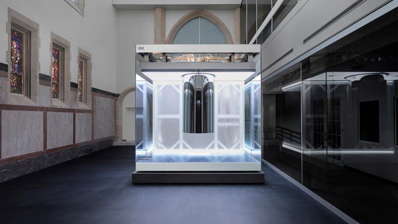
Rensselaer Polytechnic Institute and IBM Unveil the World’s first IBM Quantum System One on a University Campus
Now online, the IBM quantum system will expand the longstanding RPI and IBM partnership to accelerate quantum computing research, workforce development, and education in New York.
Latest News
Six RPI Students Receive Prestigious NSF Graduate Research Fellowships
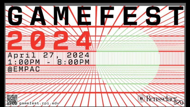
Rensselaer To Host GameFest 2024 on April 27
Rensselaer Researcher Finds that Frog Species Evolved Rapidly in Response To Road Salts
RPI To Host Panel on Sleep and Your Health April 16
Rensselaer Faculty Presents Innovative World Premiere at Troy Savings Bank Music Hall
Rensselaer Polytechnic Institute and IBM Unveil the World’s first IBM Quantum System One on a University Campus
Editor's Picks
Rensselaer Researcher Finds that Frog Species Evolved Rapidly in Response To Road Salts
Rensselaer To Host GameFest 2024 on April 27
Six RPI Students Receive Prestigious NSF Graduate Research Fellowships
Campus & Community
Image
Rensselaer’s Science and Technology Studies Department Adds Three Faculty This Academic Year
Image
Rensselaer Professor Esther Wertz Appointed UPWARDS For the Future Faculty Fellow To Support Semiconductor Education, Workforce Training, and Research
Image
Professor Jonathan Dordick Receives Two Prestigious Honors
Image
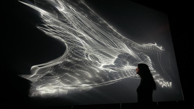
“Reverberating Light” Installation Recognized
Back to top