May 8, 2015

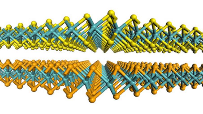
Troy, N.Y. – A $2 million grant from the National Science Foundation (NSF) will allow researchers led by Rensselaer Professor Humberto Terrones to explore the structure and capabilities of transition metal dichalcogenides, layered nanomaterials with intriguing optical and electronic properties. Transition metal dichalcogenides (TMDs), a class of materials composed of a transition metal and sulfur or selenium atoms, have potential applications as semiconductors and optical sensors. The metallic phases of TMDs can exhibit superconductivity.
“Because of the arrangement of the atoms, the material absorbs and plays with light in a particular way, reflecting or absorbing light based upon its symmetry,” said Terrones, the Rayleigh Chair for Theoretical Physics and a tenured full professor in the Department of Physics, Applied Physics, and Astronomy at Rensselaer Polytechnic Institute (RPI). “We want to investigate the properties — both linear and nonlinear optical properties — that come from these materials.”
Terrones is an expert in layered nanostructures — very thin materials, some with a thickness of only one atom – such as graphene and hexagonal boron nitiride. He performs theoretical modeling of the structural, vibrational, and electronic properties of these materials, as well as experimental synthesis and characterization, which is used to validate the models. His recent focus has been on emerging nanomaterials such as TMDs.
“Because the electronic properties in TMDs change from indirect band gap to direct gap depending on the thickness of the material, you can tune the electronic and optical properties depending on the number of layers the material exhibits,” said Terrones. “With this grant, we will be exploring the electronic properties of transition metal dichalcogenides in a mono-layer, as well as two- and three-layer materials.”
One example of a TMD is molybdenum disulfide, which can be found in nature as the crystal molybdenite. Several layers of molybdenum disulfide, even as few as two layers, act as an indirect gap semiconductor, but when reduced to a mono-layer, molybdenum disulfide becomes a direct gap semiconductor. Each of these properties offers potential applications in photovoltaics and photoelectronics.
“At the most basic level, a direct gap semiconductor may have opto-electronic applications — you can introduce a particular wavelength of light and create a current,” said Terrones. “With a direct band gap semiconductor in the visible range, you can use light to make devices work for useful applications.”
NSF Office of Emerging Frontiers in Research and Innovation awarded the grant to Terrones and colleagues at Pennsylvania State University, Virginia Polytechnic Institute and State University, and Washington University in St. Louis.
The goals of the project, titled “Crystalline Atomically Thin Layers for Photonic Applications,” are to synthesize different atomically thin two-dimensional (2-D) semiconducting layers, which possess novel properties often unavailable in their bulk counterparts, and incorporate them onto devices for novel photonic applications. The active and nonlinear photonic devices using 2-D materials can potentially create a new paradigm of optoelectronics and may lead to numerous optical information and quantum information-related applications.
The multidisciplinary team will investigate key research areas from 2-D material synthesis, condensed matter theory, and optical engineering. Although Terrones is equally interested in theory and experimentation, in this project, he will focus largely on theory.
“I will design a structure or heterostructure, model it, and calculate its properties,” said Terrones. “And I tell the experimentalists what to build and how we can expect the structure to behave.”