October 27, 2016
It’s a small change that makes a big difference. Researchers have developed a method that uses a one-degree change in temperature to alter the color of light that a semiconductor emits. The method, which uses a thin-film semiconductor layered on top of a heat-sensitive substrate material, offers a path to electronically triggering changes in the properties of semiconductor materials.
“We can change the color of the light that the material emits with only a small change in the temperature of the substrate,” said Jian Shi, an assistant professor of materials science and engineering at Rensselaer Polytechnic Institute. “If you can manipulate a material through temperature, you can also potentially manipulate it with voltage, and make an electronic device, and that is significant. Now you can control emission wavelengths electronically.”
The research is detailed in “Nonlinear Electron-Lattice Interactions in a Wurtzite Semiconductor Enabled via Strongly Correlated Oxide,” published in a recent edition of Advanced Materials.
Materials scientists like Shi develop materials with properties that can enable new technologies or better suit current technologies. In essence, there are three major options for changing the properties of a material: change the composition, change the temperature, or change the pressure on the material. Each has advantages and drawbacks, and a material suitable for commercial applications must be economical and exhibit the necessary properties under relatively common conditions.
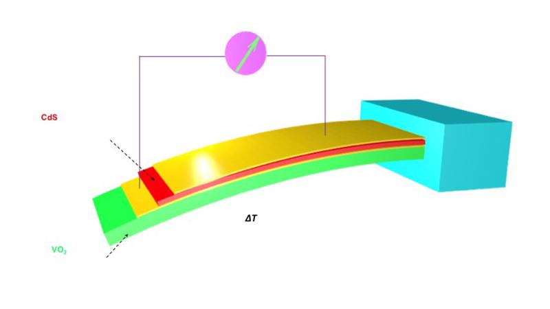
In this research, Shi focused on the use of pressure to alter the electron-lattice composition, or symmetry, of cadmium sulfite, and change its properties. The use of bulk pressure has potential pitfalls: it takes a lot of energy to change the electron-lattice interaction of a material through pressure; generating that energy may require the use of a bulky apparatus that renders the material inaccessible for applications; and many materials have little tolerance for deformation and will actually shatter before they can be deformed sufficient to provoke new properties. For example, cadmium sulfite in bulk will shatter at .1 percent deformation, which is not enough to change its electron-lattice interaction, and therefore its material properties.
To overcome those pitfalls, Shi’s approach uses a thin film of the semiconductor – which can tolerate greater deformation than the bulk material – deposited onto a substrate material that deforms substantially when subjected to only a slight temperature change. The thin film of cadmium sulfite, can tolerate at least one percent deformation without shattering, a 10-fold advantage over the bulk material. The substrate material, vanadium dioxide, undergoes a phase transformation from metal to insulator between 6 and 8 degrees Celsius, changing the volume of the material and exerting pressure on the thin film semiconductor deposited on its surface.
By combining the robust thin film semiconductor with the temperature sensitive substrate, Shi is able to easily subject the semiconductor to great strain.
The method could be extended to a variety of thin-film semiconductors and to substrates that undergo phase transition from pressure, as well as temperature, or electrostatic doping.
Significantly, the results also hint at the potential for producing a voltage from thermal energy, which could lead to harvesting thermal energy.
“If you change the lattice constant and the symmetry — of a material, sometimes you can generate energy, like a current spike,” Shi said. “If we can change thermal energy to electricity by changing the material’s symmetry, we can harvest thermal energy.”
At Rensselaer, experimental study and theoretical analysis were conducted in the laboratories of Shi, and Toh-Ming Lu, the Ray Palmer Baker Distinguished Professor of Physics, Applied Physics, and Astronomy, with the aid of doctoral candidate Yiping Wang and graduate student Lucas Seewald, and Xin Sun, a postdoctoral research associate. Researchers Jared Johnson and Jinwoo Hwang from Ohio State University prepared imaging of both the semiconducting film and phase transition substrate. This work was supported by National Science Foundation grant award CMMI 1550941.
This research fulfills the vision of The New Polytechnic, an emerging paradigm for higher education which recognizes that global challenges and opportunities are so complex, they cannot be addressed by even the most talented person working alone. Rensselaer serves as a crossroads for collaboration — working with partners across disciplines, sectors, and geographic regions, to address global challenges — and addresses some of the world’s most pressing technological challenges, from energy security and sustainable development to biotechnology and human health. The New Polytechnic is transformative in the global impact of research, in its innovative pedagogy, and in the lives of students at Rensselaer.
About Rensselaer Polytechnic Institute
Rensselaer Polytechnic Institute, founded in 1824, is America’s first technological research university. The university offers bachelor’s, master’s, and doctoral degrees in engineering; the sciences; information technology and web sciences; architecture; management; and the arts, humanities, and social sciences. Rensselaer faculty advance research in a wide range of fields, with an emphasis on biotechnology, nanotechnology, computational science and engineering, data science, and the media arts and technology. The Institute has an established record of success in the transfer of technology from the laboratory to the marketplace, fulfilling its founding mission of applying science “to the common purposes of life.” For more information, please visit http://www.rpi.edu.