December 16, 2019
The vast number of devices that rely on technologies such as optic fibers, electric circuits, and sensors could be faster, more efficient, and more effective if the materials used to make them were improved.
In Nano Letters, researchers from Rensselaer Polytechnic Institute recently demonstrated how they could harness promising characteristics of one such material — vanadium dioxide (VO2) — in order to lay the groundwork for practical application in future technologies.
VO2 has long been eyed for its ability to easily transition from a metal to an insulator, and back, with a simple application of voltage, light, or temperature. The material’s weakness was its inability to adequately be grown on silicon — a necessary integration if it’s to be used within electronics.
“In the past, whenever you wanted to grow VO2 on silicon, you couldn’t create a good quality material. The reason is what we call a lattice and chemistry mismatch,” said Jian Shi, an associate professor of materials science and engineering at Rensselaer. “They don’t match each other, so if you try to match them together, then you would have other defects. You would produce a very lousy material.”
Shi said researchers knew they could grow a good quality version of VO2 on other materials, like sapphire, for example. Sapphire, however, isn’t as useful as silicon for electronics.
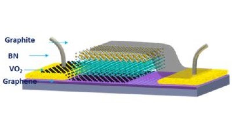
The Rensselaer team took this knowledge and tried a new approach. The researchers applied a very thin layer of graphene to sapphire before trying to grow the VO2. The graphene acted as a buffer and allowed the researchers to peel off the graphene and VO2 combination, after growth, so they could transfer it onto silicon in order to build a device. The existence of a buffer layer of graphene did not disrupt the lattice relationship between VO2 and sapphire after growth. This process is called “remote epitaxy.”
“This is the first demonstration of this method, with this compound,” Shi said.
What they also found was that growing VO2 in this way actually produced a better quality material. The graphene buffer added more value than the researchers even anticipated.